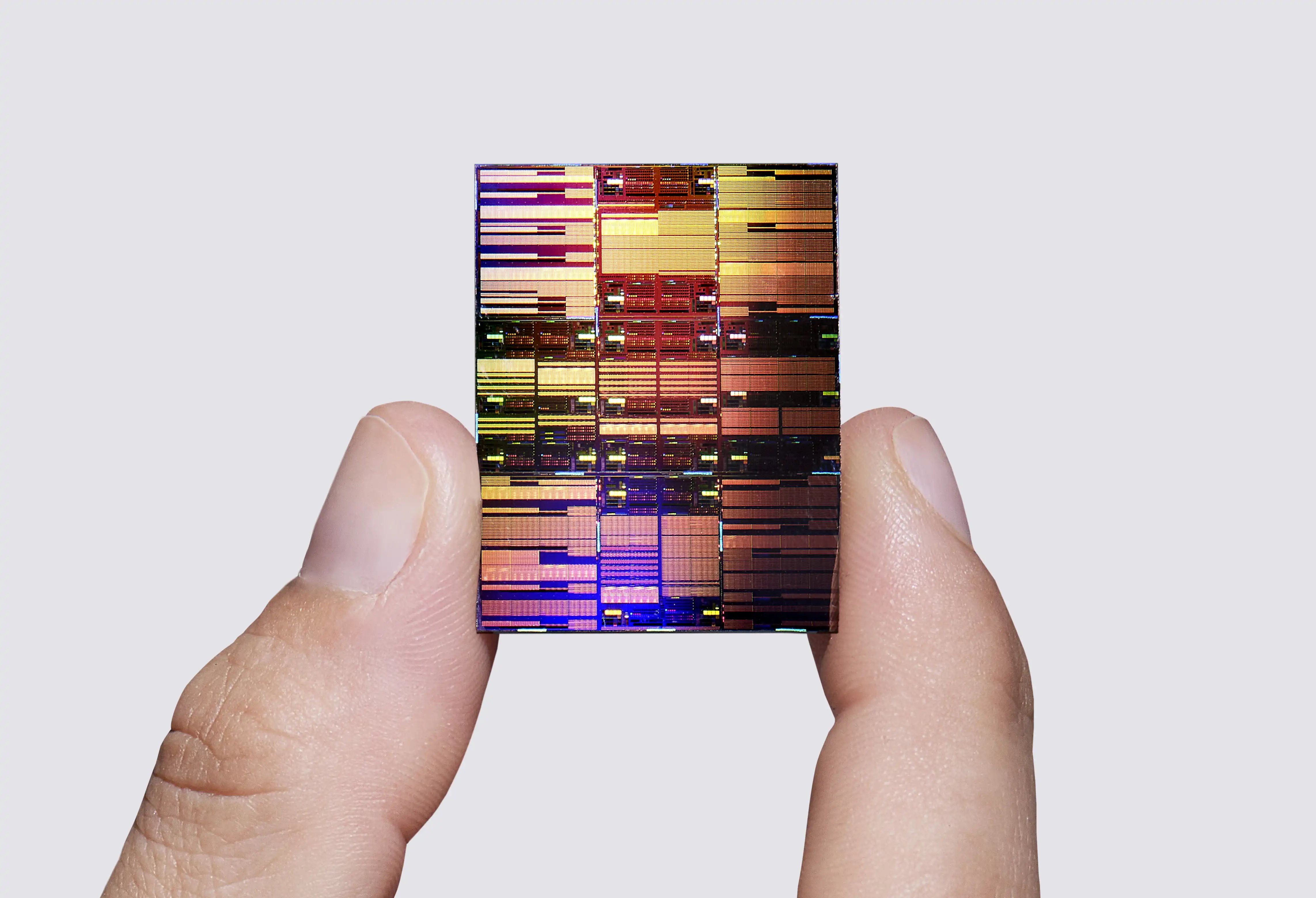
IBM has unveiled a new semiconductor technology that promises a significant leap forward in chip performance and energy efficiency. The company claims its "0.7-nanometer" technology can deliver computer chips with 50% better performance and 70% greater energy efficiency compared to its 2-nanometer chips. IBM's new chip technology could enable faster smartphones and laptops, more efficient data centers, better self-driving cars, and more capable AI tools.
The nanometer, an atomic-scale unit of measurement, refers to how densely transistors—the tiny electronic switches that make up processors—can be packed together. The smaller the number, the more transistors can fit on a chip the size of a fingernail. IBM's new technology packs nearly 100 billion transistors onto a chip that size—nearly twice the density of the 2-nanometer chip. This advancement could help address the tech industry's growing energy needs while cramming more computing power into smaller devices.
IBM's breakthrough uses a new three-dimensional architecture called "nanostack," which stacks transistor layers on top of each other rather than arranging them in a single layer. This nanostack architecture vertically stacks transistors in a staggered layout to pack more transistors into the same chip space. The basic unit of IBM's nanostack architecture consists of two transistors stacked and bonded together, each consisting of three nanosheets that are individually 5 nanometers thick.
While the technology isn't ready for mass production yet, IBM expects to reach the manufacturing stage within five years. The company doesn't manufacture chips itself, instead licensing its designs to companies. It has partnered with semiconductor companies such as Japan's Rapidus to mass manufacture its previous generation of 2-nanometer node chips.
As the company moves towards mass production, the impact of this breakthrough on consumer devices, data centers, and AI applications will be closely watched.
IBM has unveiled a new semiconductor technology that promises a significant leap forward in chip performance and energy efficiency. The company claims its "0.7-nanometer" technology can deliver computer chips with 50% better performance and 70% greater energy efficiency compared to its 2-nanometer chips. This breakthrough could have wide-ranging implications for the tech industry, from faster smartphones and laptops to more efficient data centers and advanced AI tools.
The nanometer, an atomic-scale unit of measurement, refers to how densely transistors—the tiny electronic switches that make up processors—can be packed together. The smaller the number, the more transistors can fit on a chip the size of a fingernail. IBM's new technology packs nearly 100 billion transistors onto a chip that size—nearly twice the density of the 2-nanometer chip. This advancement could help address the tech industry's growing energy needs while cramming more computing power into smaller devices.
IBM's breakthrough uses a new three-dimensional architecture called "nanostack," which stacks transistor layers on top of each other rather than arranging them in a single layer. This nanostack architecture vertically stacks transistors in a staggered layout to pack more transistors into the same chip space. The basic unit of IBM’s nanostack architecture consists of two transistors stacked and bonded together, each consisting of three nanosheets that are individually 5 nanometers thick.
While the technology isn't ready for mass production yet, IBM expects to reach the manufacturing stage within five years. The company doesn't manufacture chips itself, instead licensing its designs to companies. It has partnered with semiconductor companies such as Japan's Rapidus to mass manufacture its previous generation of 2-nanometer node chips. IBM declined to name specific companies that it may partner with to commercialize the newest sub-1-nanometer node technology but expects commercial chips incorporating the newest nanostack architecture could begin production as early as in the next five years and most likely within a decade.
IBM's new chip technology represents a significant advancement in the semiconductor industry, promising higher-performance, low-power chips that could transform various tech sectors. As the company moves towards mass production, the impact of this breakthrough on consumer devices, data centers, and AI applications will be closely watched.
Highlighted text was flagged by the council. Tap to see feedback.